
Introduction to Kingdta Electronics
If you are looking for a reliable partner to take your electronics from prototype to mass production, Kingdta Electronics stands out as a professional one-stop PCBA manufacturer with proven capacity, digitalized quality control, and global delivery experience. Founded in 2011, Kingdta has grown into a comprehensive ODM/OEM provider that integrates PCB manufacturing, full BOM component sourcing, SMT and DIP assembly, testing, programming, coating, and final product assembly. With ISO 9001 certification, RoHS compliance, and CE/UL capability, our customers in automotive, new energy, industrial, medical, communications, security, consumer, commercial display, and smart home fields trust us for consistent quality and on-time delivery.
One-Stop PCBA Services Built for Speed and Reliability
Turnkey PCBA Coverage
- PCB fabrication and layout review
- Full BOM component procurement (turnkey, customer-supplied, or hybrid)
- SMT assembly (including 01005 components and high-precision placement)
- THT/DIP assembly and double wave soldering
- Programming and burn-in
- AOI, ICT/FCT, and functional testing
- Conformal coating, product assembly, and custom packaging
By consolidating critical steps under one roof and integrating MES (Manufacturing Execution System), Kingdta enables rapid prototyping and stable mass production with complete traceability—from raw materials to shipment.
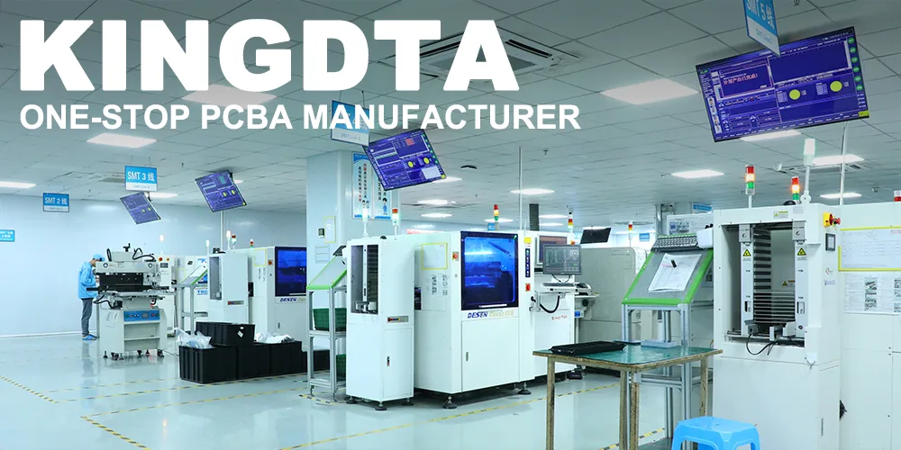
Manufacturing Scale and Equipment You Can Trust
Production Lines and Core Equipment
- 7 SMT production lines equipped with multi-functional high-speed placement machines (including Yamaha), automatic solder paste printers, SPI inspection, and dual-lane nitrogen reflow ovens
- 3 DIP plug-in lines supporting through-hole assembly with double wave solder machines
- 2 assembly lines for product-level integration, coating, and verification
- Critical inspection and reliability tools: AOI, X-ray for BGA inspection, first article testers, ICT/FCT setups, and aging systems
This robust setup enables high-volume throughput while maintaining consistent quality standards. Whether you are scaling a new product introduction (NPI) or stabilizing mass production, Kingdta’s equipment and processes deliver predictable outcomes.
Advanced Process Capabilities for Complex Designs
Precision and Board Specifications
- Minimum line width/spacing: approximately 60 μm
- Minimum component size: 01005; placement accuracy up to ±0.03 mm
- Minimum pin pitch: 0.25 mm for fine-pitch packages
- PCB size: up to 610 × 520 mm; layers: 1–16
- Copper thickness: up to ~120 μm; board thickness: 0.3–2.0 mm
- Packaging expertise: BGA, QFN, QFP, SOP, CSP (upon evaluation), with X-ray verification for BGA integrity
These capabilities allow us to handle high-density, high-performance boards common in automotive, medical, and industrial applications.
Digitalized Quality Control with MES
End-to-End Traceability and Quality Gates
- End-to-end traceability of materials, processes, and test results
- Real-time quality gates with error-proofing and leakage prevention
- Full visibility into process data for audits and continuous improvement
Our quality flow typically includes incoming material inspection, custom stencil fabrication, first article validation, SPI, SMT, controlled reflow with furnace profiling, AOI, X-ray, ICT/FCT functional testing, aging, OQC, and shipment. For thermal process control, we use 9-channel furnace profiling (typical: 260°C <10s, 235°C for 60–90s) to ensure robust solder joints across complex assemblies.
Smart Warehousing and Component Integrity
Moisture, Counting, and Prebake Controls
- 20% RH moisture-proof cabinets for ICs and moisture-sensitive parts
- X-ray counting machines for accurate, non-destructive inventory control
- 500× microscope verification to screen silks and monitor oxidation
- Mandatory 24-hour prebake for PCBs, BGA, and moisture-sensitive materials prior to production
This disciplined approach minimizes defects, prevents ESD risks, and stabilizes process yields, especially for advanced packages and high-density assemblies.
Flexible Sourcing Models and Cost Optimization
Turnkey, Hybrid, and DFM-Driven Savings
- Full BOM component procurement to streamline logistics and reduce lead time
- Customer-supplied or hybrid sourcing models to fit your supply chain strategy
- BOM optimization, footprint validation, and panelization recommendations to maximize yield and minimize waste
For many customers, our turnkey model enables “zero inventory” on their side, while our procurement team ensures long-term supply continuity for critical components.
Lead Times and Global Delivery
Rapid Prototyping and Predictable Mass Production
- Rapid prototyping for PCBA—often as fast as 7 days
- Mass production lead times of approximately 14–22 days, depending on BOM complexity and material readiness
- Experience delivering to Asia, Europe, and the Americas with reliable logistics and documentation
Our location in Shenzhen’s Bao’an District provides convenient access to the global electronics supply chain, allowing us to source components efficiently and ship finished goods quickly.
Industries We Serve
From Automotive to Smart Home
- Automotive electronics and EV-related systems
- New energy solutions and power management
- Industrial control and automation
- Medical devices and instrumentation
- Communications and networking
- Security and surveillance
- Consumer electronics and IoT devices
- Commercial displays and smart home products
From prototype validation to ramping production, we tailor our process windows and test strategies to meet industry-specific standards and compliance requirements.
Why Partner with Kingdta Electronics
Key Reasons to Choose Kingdta
- Proven one-stop PCBA capability for ODM/OEM projects
- ISO 9001 certification, RoHS compliance, and CE/UL capability
- MES-driven traceability and process control
- Advanced SMT/THT with nitrogen reflow, double wave solder, AOI, X-ray
- High-precision assembly down to 01005 and 0.25 mm pitch
- Cost-effective DFM and turnkey BOM sourcing
- Fast prototyping and predictable mass production timelines
- Dedicated engineering support and clear documentation
Get Started with Kingdta
Whether you’re refining a prototype or scaling to volume, Kingdta Electronics delivers speed, quality, and confidence. Contact us to discuss your PCB/PCBA requirements, request a free quote, or schedule a factory walkthrough. We’re ready to help you turn great designs into reliable products—efficiently and at scale.